The pain points in producing custom-made small-sized solar panels (typically referring to those ranging from tens of milliwatts to several watts, used in IoT devices, sensors, consumer electronics, etc.) mainly lie in balancing process, cost, efficiency, and reliability.
 Three major pain points
Pain Point 1:
Three major pain points
Pain Point 1: The main busbar design (dot/segmented) of mainstream large-size solar cells leads to significant waste during small-size cutting.
Background
- Currently, mainstream large-size solar cells (182mm×182mm, 210mm×210mm) generally adopt a multi-busbar (MBB, 9BB~18BB) design with discontinuous "segmented" or "dot" busbar lines to reduce silver loss and improve efficiency.
- There are no metal electrodes between these busbars.
Impact on Small-Size Cutting
- When you cut multiple smaller wafers (e.g., to 20mm×20mm or even smaller) from a large solar cell:
- The smaller wafers are likely to fall into the metal-free areas between the busbar lines, resulting in a lack of complete busbars for soldering or conduction.
- Even if the busbar positions are aligned as much as possible during cutting, it still results in wafer-level layout waste—many areas cannot become effective wafers, and the overall utilization rate may only be 40~60%.
Compared to older solar cells
In the past, small-sized solar cells (such as 156mm or 125mm) mostly had continuous through-type main grid lines. When cutting the cells into smaller pieces, current could be drawn out as long as a section of the main grid was included. This was much more flexible than the current segmented design.
Pain Point 2: Reduced Solar Cell Thickness (220μm → 140μm or even thinner) Leads to a Sharp Drop in Process Yield
Background
- To reduce costs and improve efficiency (thinner cells shorten carrier transport paths and reduce recombination), the mainstream thickness of solar cells has decreased from 220μm a decade ago to 140μm now, and some TOPCon/HJT cells are even moving towards 130μm and 110μm.
Specific Impact on Small-Size Customization
Manufacturing process
|
Pain Point Explanation
|
|
Laser cutting (dicing) |
Thin solar cells are more sensitive to thermal stress and are prone to microcracks or even dark cracks at the cut edges. The proportion of cracks increases significantly when cutting in small batches.
|
|
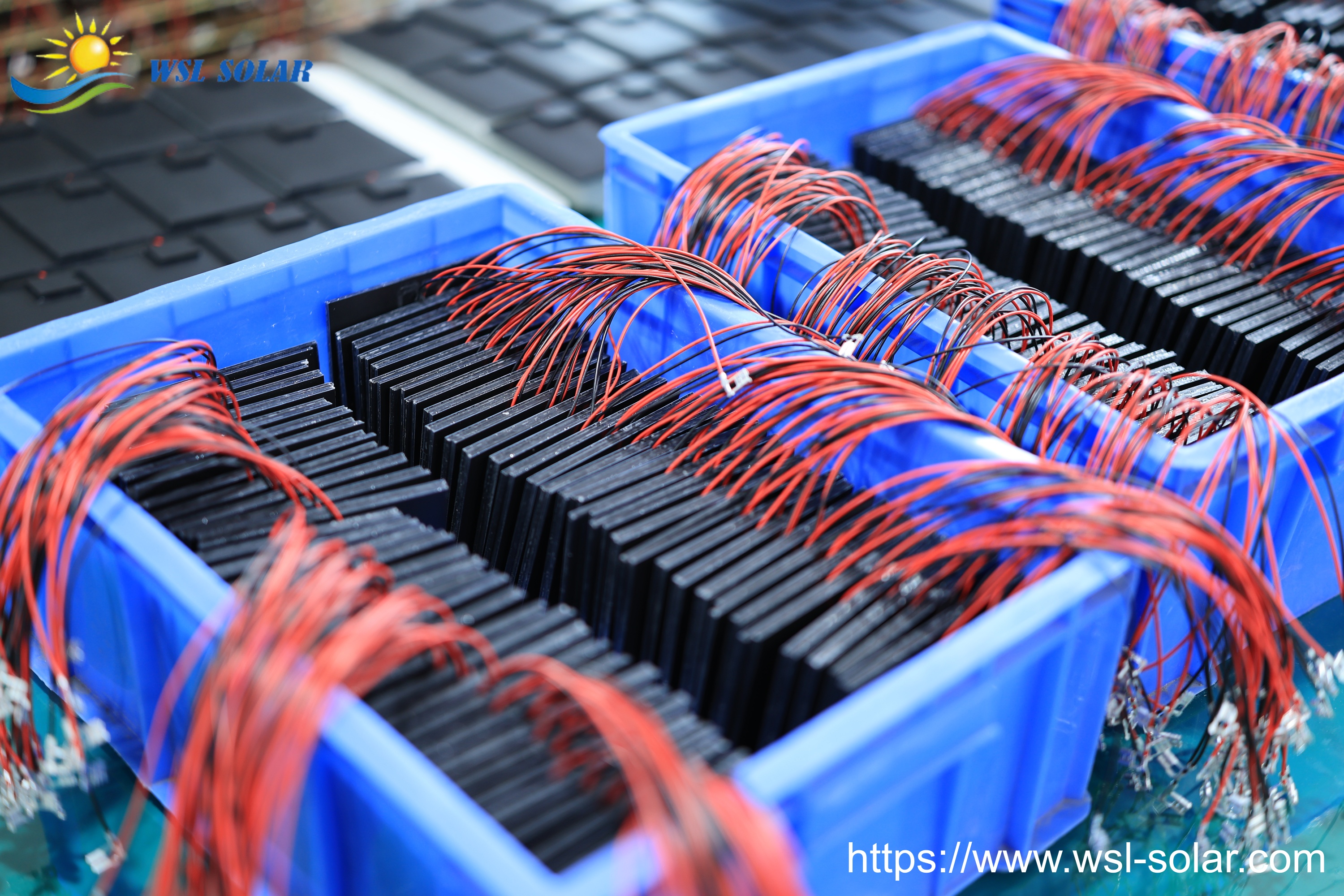
String welding (manual or semi-automatic) |
Thin solar cells have a small heat capacity, and localized thermal shock during soldering or infrared heating can easily cause them to break. Furthermore, the small surface area exposed to stress means they will shatter even with slightly higher soldering pressure.
|
|
Lamination and stacking |
Thin solar cells are more prone to microcracks or displacement during lamination due to the flow thrust of EVA/POE and vacuum pressure. This problem becomes even more pronounced when there are many small-sized cells.
|
Results
In the past, during the 220μm era, the overall yield of customized small sizes could reach 90~95%; now, with 140μm, the actual yield of many factories fluctuates between 70~85%.
Pain Point 3: Insufficient Reliability of Foldable/Portable/Non-Glass Encapsulation (Poor Shock Resistance, Poor Water Resistance)
Common Solutions
- These products typically use ETFE (fluoroplastic film) + composite material backsheet (such as PET/fabric) + flexible crystalline silicon solar cells, with back-contact solar cells or flexible thin-film solar cells (CIGS/a-Si).
- The aim is to be lightweight, bendable, non-glass, and easy to carry.
Actual Problems Exposed
Reliability dimension
|
Specific manifestations
|
|
Impact resistance |
ETFE has a surface hardness much lower than glass. When scratched by sharp objects (keys, branches, backpack zippers), its light transmittance decreases and it is easily penetrated by moisture. Small crystalline silicon wafers may develop microcracks or even shatter after being subjected to point impacts.
|
|
Waterproof |
Edge sealing usually relies on hot melt adhesive or structural adhesive. After repeated folding or temperature changes (-20℃~60℃), the adhesive layer fatigues and cracks, allowing moisture to enter from the side or lead-out position, leading to EVA hydrolysis, electrode corrosion, and rapid power decay.
|
|
interlayer delamination |
The CTE (coefficient of thermal expansion) between the flexible encapsulation material and the crystalline silicon wafer is large. After several months of outdoor day and night cycling, bubbles and delamination appear, and the appearance turns white.
|
In summary, these three major pain points directly address the structural contradictions arising from the evolution of crystalline silicon technology towards larger sizes, thinner wafers, and finer grids, and the demand for customized small-size wafers.
- Incompatibility in solar cell design: The segmented grids of large solar cells prevent the cutting of complete electrodes for small-size wafers;
- Approaching physical limits: The yield of thin solar cells is uncontrollable in miniaturization processes;
- Lack of encapsulation systems: Non-glass solutions lack industrially mature, low-cost, and highly reliable structures.
Posted by Carrie Wong / WSL Solar
WSL Solar has been a quality and professional manufacturer of
custom solar panels, solar mini panels, IoT solar panels and solar solution provider in China since 2006.
https://www.wsl-solar.com